Microstrip tee junction

A model of a microstrip tee junction is published in [36]. Figure 11.8 shows a unsymmetrical microstrip tee with the main arms consisting of port a and b and with the side arm consisting of port 2. The following model describes the gray area. The equivalent circuit is depicted in figure 11.9. It consists of a shunt reactance $ B_T$, one transformer in each main arm (ratios $ T_a$ and $ T_b$) and a microstrip line in each arm (width $ W_a$, $ W_b$ and $ W_2$).

Figure 11.8: unsymmetrical microstrip tee (see text)
\includegraphics[width=7cm]{mstee2}

Figure 11.9: equivalent circuit of unsymmetrical microstrip tee
\includegraphics[width=13cm]{mstee}

First, let us define some quantities. Each of them is used in the equations below with an index of the arm they belong to ($ a$, $ b$ or $ 2$).

equivalent parallel plate line width:$\displaystyle \qquad D = \frac{Z_{F0}}{\sqrt{\varepsilon_{r,eff}}} \cdot \frac{h}{Z_L}$ (11.207)

where $ Z_{F0}$ is vacuum field impedance, $ h$ height of substrate, $ \varepsilon_{r,eff}$ effective, relative dielectric constant, $ Z_L$ microstrip line impedance.

first higher order mode cut-off frequency:$\displaystyle \qquad f_p = 4\cdot 10^5 \cdot\frac{Z_L}{h}$ (11.208)

effective wave length of the microstrip quasi-TEM mode:$\displaystyle \qquad \lambda = \frac{c_0}{\sqrt{\varepsilon_{r,eff}}\cdot f}$ (11.209)

The main arm displacements of the reference planes from the center lines are (index $ x$ stand for $ a$ or $ b$):

$\displaystyle d_x = 0.055\cdot D_2\cdot \frac{Z_{L,x}}{Z_{L,2}}\cdot \left( 1 - 2\cdot\frac{Z_{L,x}}{Z_{L,2}}\cdot \left( \frac{f}{f_{p,x}} \right)^2 \right)$ (11.210)

The length of the line in the main arms is:

$\displaystyle L_x = 0.5\cdot W_2 - d_x$ (11.211)

where $ f$ is frequency.

The side arm displacement of the reference planes from the center lines is:

$\displaystyle d_2 = \sqrt{D_a \cdot D_b}\cdot \left( 0.5 - R\cdot \left( 0.05 +...
...\left(-1.6\cdot R\right) + 0.25\cdot R\cdot Q - 0.17\cdot \ln R \right) \right)$ (11.212)

The length of the line in the side arm is:

$\displaystyle L_2 = 0.5\cdot$   max$\displaystyle \left(W_a, W_b\right) - d_2$ (11.213)

where max$ \left(x, y\right)$ is the larger of the both quantities, $ R$ and $ Q$ are:

$\displaystyle R = \frac{\sqrt{Z_{L,a}\cdot Z_{L,b}}}{Z_{L,2}} \qquad Q = \frac{f^2}{f_{p,a}\cdot f_{p,b}}$ (11.214)

Turn ratio of transformers in the side arms:

$\displaystyle T_x^2 = 1 - \pi\cdot \left( \frac{f}{f_{p,x}} \right)^2 \cdot \le...
...ac{Z_{L,x}}{Z_{L,2}} \right)^2 + \left( 0.5 - \frac{d_2}{D_x} \right)^2 \right)$ (11.215)

Shunt susceptance:

\begin{displaymath}\begin{split}B_T &= 5.5\cdot \sqrt{\frac{D_a\cdot D_b}{\lambd...
...dot \left( \frac{Z_{L,2}}{Z_{F0}} \right)^2 \right) \end{split}\end{displaymath} (11.216)

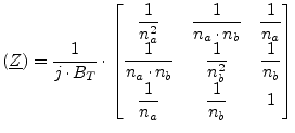
For better implementation of the microstrip tee (figure 11.9) the device parameter of the internal equivalent circuit (two transformers and the shunt susceptance) are given below. The port numbering for them is port a = 1, port b = 2 and port 2 = 3.

$\displaystyle (\underline{Y}) =$   infinity (11.217)

$\displaystyle (\underline{Z}) = \frac{1}{j\cdot B_T}\cdot \begin{bmatrix}\dfrac...
...n_b^2} & \dfrac{1}{n_b} \\ \dfrac{1}{n_a} & \dfrac{1}{n_b} & 1 \\ \end{bmatrix}$ (11.218)

$\displaystyle \underline{S}_{11} = \frac{1 - n_a^2\cdot (j\cdot B_T\cdot Z_0 + \frac{1}{n_b^2} + 1)} {1 + n_a^2\cdot (j\cdot B_T\cdot Z_0 + \frac{1}{n_b^2} + 1)}$ (11.219)

$\displaystyle \underline{S}_{22} = \frac{1 - n_b^2\cdot (j\cdot B_T\cdot Z_0 + \frac{1}{n_a^2} + 1)} {1 + n_b^2\cdot (j\cdot B_T\cdot Z_0 + \frac{1}{n_a^2} + 1)}$ (11.220)

$\displaystyle \underline{S}_{33} = \frac{1 - \left( \frac{1}{n_a^2} + \frac{1}{...
...)} {1 + \left( \frac{1}{n_a^2} + \frac{1}{n_b^2} + j\cdot B_T\cdot Z_0 \right)}$ (11.221)

$\displaystyle \underline{S}_{13} = \underline{S}_{31} = \frac{2\cdot n_a}{n_a^2\cdot \left( \frac{1}{n_b^2} + j\cdot B_T\cdot Z_0 + 1\right) + 1}$ (11.222)

$\displaystyle \underline{S}_{23} = \underline{S}_{32} = \frac{2\cdot n_b}{n_b^2\cdot \left( \frac{1}{n_a^2} + j\cdot B_T\cdot Z_0 + 1\right) + 1}$ (11.223)

$\displaystyle \underline{S}_{12} = \underline{S}_{21} = \frac{2}{n_a\cdot n_b\cdot \left( j\cdot B_T\cdot Z_0 + 1\right) + \frac{n_a}{n_b} + \frac{n_b}{n_a}}$ (11.224)

The MNA matrix representation can be derived from the Z parameters in the following way.
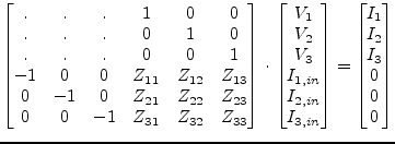
$\displaystyle \begin{bmatrix}. & . & . & 1 & 0 & 0\\ . & . & . & 0 & 1 & 0\\ . ...
... \end{bmatrix} = \begin{bmatrix}I_{1}\\ I_{2}\\ I_{3}\\ 0\\ 0\\ 0 \end{bmatrix}$ (11.225)

Please note that the main arm displacements in eq. (11.210) yield two small microstrip lines at each main arm and the side arm displacement of eq. (11.212) results in a small microstrip strip line as well, but with negative length, i.e. kind of phaseshifter here.

The transformer ratios defined in eq. (11.215) are going to be negative with increasing frequency which produces complex values in the Z-parameter matrix as well as in the S-parameter matrix. That is why the ratios are delimited to a minimum value.


This document was generated by Stefan Jahn on 2007-12-30 using latex2html.